You can download the sample Engineering Assignment on Microcontroller with the following question for free at the end of this page. For further assistance in Engineering Assignment help, please check our offerings in Engineering assignment solutions. Our subject-matter experts provide online assignment help to Engineering students from across the world and deliver plagiarism free solution with free Turnitin report with every solution.
(AssignmentEssayHelp does not recommend anyone to use this sample as their own work.)
Engineering Assignment Question
- You are part of the R&D team in leading Audio Company, Sound-Spark. The company has just decided to create its first MP3 player. As the lead designer, you have been given the responsibility to evaluate the MC68HC11 as a possible CPU for the MP3 Player. Your are to submit a report that should include the following
- Advantages of using the MC68HC11
- Block Diagram Stating the connections of the microprocessor to other components
- Evaluate the other components that may be needed for the design, such as memory, input buttons, display and so on.
- Disadvantages / Difficulties of using the MC68HC11 and any suggestions to overcome them.
Outcome: 1.2
- Suggest 3 other application for micro controllers. For your suggestions, do you think that the 68HC11 is good candidate to be the micro controller? Justify your answer.
Engineering Assignment Solution
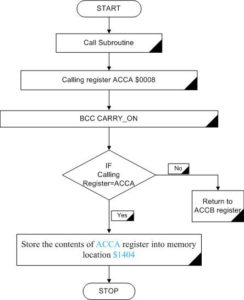
The subroutine is executed in order to make the stack register store the current address temporarily so that it can be recovered at a later point in the program. The addresses are restored to the PC in the reverse order called a stack to which they were stored, that is, 'last in, first out' (LIFO), like a stack of plates. Subroutines are used to carry out discrete program functions.
To set the serial link’s baud rate, BAUD register is used and contains two control bits for factory testing. There are two control registers in MC68HC11, SCCR1 and SCCR2 that specify that how the SCI should work. SCCR1 includes three bits associated with the optional 9-bit data format. The WAKE bit is used to select one of two methods of the receiver to wake up. SCCR2 contains the main SCI controls. The upper four bits are used for local interrupt enable controls, which determine whether SCI status flags will be polled or will generate hardware interrupt requests. The TE and RE bits are the respective transmitter and receiver subsystem enables controls. The RWU bit allows software to put the receiver to sleep and hardware to automatically wake it up by clearing this bit. The send break SBK bit allows software to generate break characters on the TxD line.
There is a status register, SCSR that can be used by the programmer to check whether the transmission/reception of a frame has been completed or not. The SCSR contains two transmitter status flags and five receiver-related status flags.
The transmitter generates flags for TDRE and TC. The receiver generates flags for RDRF, OR, idle-line detect (IDLE), a noise flag (NF), and a framing error (FE) indication. Finally, there is the data register SCDR that holds the transmitted or received information bits in MC68HC11. The SCDR is actually two separate registers. TDR is a write-only transmit data buffer register, and RDR is a read-only receive data buffer register. When software reads SCDR, it is accessing RDR; when software writes to SCDR, it is accessing TDR.
- Explain the ports that are available on the 68HC11. What can the ports be used for?
The MC68HC11A8 has a total of 40 I/O pins. All these pins are shared between general-purpose I/O usage and at least one other on-chip peripheral function.
Port A includes general-purpose I/O, the main timer system, and the pulse accumulator system. Port A has three fixed-direction input pins, four fixed direction output pins, and one bidirectional pin. The direction of the PA7 pin is controlled by the data direction register A bit 7 control bit (DDRA7) in the pulse accumulator control (PACTL) register. Port A data is read from and written to the PORTA register. Meaningful data may be read from port An even when the pins are configured to an alternate timer or pulse accumulator function. Data written to port A does not directly affect port A pins configured for an alternate timer output function, but the data is remembered in an internal latch so that, if the alternate function is disabled later, the last data written to port A will be driven out of the associated output pin.
Ports B and C and the strobe A (STRA) and strobe B (STRB) pins should be considered together because their function depends on the basic operating mode of the MC68HC11A8.
When the microcontroller unit (MCU) is operating in a single-chip mode, these 18 pins are used for general-purpose I/O and for the handshake I/O subsystem.
When the MCU is operating in an expanded mode, these pins are used for a multiplexed address/data bus. The handshake and general-purpose I/O functions, which are lost in the expanded mode, can be regained by use of the MC68HC24 port replacement unit. Special care was taken in designing both these parts so that software could be developed on an expanded system using these two parts and then later be mask programmed into the read-only memory (ROM) of an MC68HC11A8, which will be used in single-chip mode. Although care was taken to assure that the expanded system with an MC68HC24 would work exactly like the MC68HC11A8 in single-chip mode, there are a few subtle differences. For the vast majority of applications, these differences are irrelevant.
Port B is a general-purpose, 8-bit, fixed-direction output port. Writes to the port B register (PORT B) cause data to be latched and driven out of the port B pins. Reads of PORT B return the last data that was written to port B. When the handshake I/O subsystem is operating in simple strobed mode, writes to PORTB automatically cause a pulse on the STRB output pin. The simple strobe mode is selected by the handshake (HNDS) control bit equal to zero in the parallel I/O control (PIOC) register.
Port C is a general-purpose, 8-bit, bidirectional I/O port. The primary direction of data flow at each port C pin is independently controlled by a corresponding bit in the data direction control register for port C (DDRC). In addition to normal I/O functions at port C, there is an independent, 8-bit, parallel latch that captures port C data whenever a selected active edge is detected on the STRA input pin. Reads of PORTCL return the contents of this port C latch; whereas, reads of PORTC return the current data from port C. Writes to either PORTC or PORTCL cause the written data to be driven out of port C output pins; however, PORTCL writes also trigger output handshake sequences; PORTC writes do not. Writes to port C pins not configured as outputs do not cause data to be driven out of those pins, but the data is remembered in……………….
(Some parts of the solution has been blurred due to privacy protection policy)


 WhatsApp Us